My Summary and Most Interested Topic in Advanced Computer Organization 2 Master's Course
1. Introduction
This lecture was intended for Master Students on 2015 Fall Semester held at Graduate School of Science and Technology, Department of Computer Science and Electrical Engineering, Kumamoto University. The lecture was delivered by Associate Professor Morihiro Kuga of Computer Architecture Lab, and followed by 12 international students. The lecture begins with the fundamental topics of representation of information, logic circuit, hardware description language (HDL) design and Verilog HDL, 24-hour digital clock design, and then microprocessor behavior and its design. After the fundamentals the lecture explains about hardware algorithms of arithmetic unit, hardware sorter, array processor and systolic array, functional memory and content addressable memory, and interconnection network. This is my own summary regarding to the lecture about how computer hardware works and who knows it might give you a description of what is inside the lecture or it might not be able to give description to you due to its difficulty. This summary is personally written by me and I license it as customized creative common share-alike (CC-BY-SA) where anyone may share, reuse, republish, and sell with the condition to state my name as the original author and mention the open and original version available here and the source codes in Github are licensed under General Public License 3.0 though they are just tutorial codes and nothing more.
2. The Fundamentals
The very first part of the lecture is to know what mathematic form information takes place and how the computer can receive, process, and output the information. In mathematics, information in the real world can be described as an analog signal. For example a sound is a 1D analog signal and image is 2D analog signal. For analog signal the precision is almost infinite (ideally) where each indicator has its own value. For computer however doesn’t directly process analog signal. The signal will be perceive by a sensor with not all the information is captured. Instead it took samples of the information and became what it is known as discrete signal. For computer today that is based on electrical the main representative value is “1” and “0”, thus for discrete signal to be represented with ones and zeros are called digital signals. For an analog signal to be converted into digital signal mainly it goes through sampling and quantization process, through analog to digital (AD) converter that outside information enters the computer. Reversely to output the information the computer uses digital to analog (DA) converter. Since it’s mainly “1”s and “0”s how to perform calculations of binary values are taught (the values we’re familiar of are decimal values “1-9”). Arithmetic calculation of binary values of addition, subtraction, multiplication, and division. The very basics of binary operation on electrical devices were introduced using clocks, shift registers, and logic gates. Many algorithms were developed which each have their own calculation speed that determines the processing power of the device.
The second topic is hardware description language (HDL), it is a specialized computer programming language used to program the design, operation, and structure of electronic circuits mostly digital circuits. It allows automated analysis and simulation of electronic circuit, and also supports compilation into lower level specification of physical electronic components. HDL looks similar to C and Pascal, a textual description programming language that consists of expressions, statements, and control structures, with the difference that HDL includes clock timing into account. A program that was introduced here was Verilog HDL, verilog is verify & logic. Verilog starts from a begin module and an end module. It uses 2 types of assignments operator blocking “=” and non blocking “<=”. Verilog’s concept consists of signal values of state “0”, “1”, “floating”, and “undefined”, and signal strengths “weak”, “strong”, etc. A subset of statements in Verilog language are synthesizeable, meaning can be physically realized by a synthesis software. Synthesis software transforms Verilog’s source into netlist (AND, OR, NOT, flip-flops, etc), that are available in a specific FPGA or VLSI technology. We practiced on 24 hour digital clock design.
The last of the fundamental topic is microprocessor and high speed technique. In computer microprocessors are implemented as a central processing unit (CPU) by integrated circuit. The CPU carries out instructions of a computer program. One of the first computer processor developed was i4004 by Intel on 1971 that has 2300 transistors, gate length of 10µm, and frequency around 108kHz. Microprocessor had greatly advanced since then, on 2007 Core2 Quad had 27000 times the frequency which is 3GHz, contains 350000 times more transistors (820000000), and shorter gate length around 45nm. As processors was able to process faster, it consumes larger power which is today’s challenge for researchers. Other vendors for microprocessors are Motorola, Mostechnology, Stanford MIPS, UCB RISC I/II, SUN Sparc, ARM, and Renesas.
Data processing on microprocessor is executed by the following order instruction fetch, decode, execute, memory, and write (FDEMW). Instructions are represented by 0 and 1, another name for this is the machine language which is very hard to understand. On top of that is assembly language that we can understand more (above that is high level programming like Pascal and C, a compiler translates high level programs to assembly, then converts assembly to machine language). We can write with assembly language like “movlw” that writes to the W register, and “movwf” after writing to W register, writes it to address of data memory. An assemble translates assembly language into machine language. Another instruction is “addwf” that add W register value and addressed of data memory and write the result to W register. There are more instructions but they usually follow the FDEMW stages.
Speaking of FDEMW there’s a method called pipelining where these stages are executed in parallel. This pipelining is said to be one of the main reason why FPGA and VLSI are fast. Without pipelining each instructions are executed in serial (one by one), but using pipelining for example “F” finishes with instruction 1, instruction 1 will continue to “D”, but at the same time “F” can be run for instruction 2, and so on. The whole point of pipelining is to make full use of the resources, minimizing the idles as much as possible. Even this pipelining had developments. Multi-pipelining uses more than one pipeline, super scalar for example. Super pipelining further divides/breaks the FDEMW process and enables pipelining in each sub process. Another one is very long instruction word (VLIW) where FDEMW can run multiple operations. This pipelining improves performance but there are also factors that prevents improvements like data dependency. Data dependency is a case where an instruction cannot be run unless a certain instruction is run first, in other words prevents parallel execution. Data dependencies can be flow dependency and vice versa (anti dependency), input dependency, output dependency, and control dependency. There are few methods to data dependencies such as handling, scheduling, and prediction. In the end all of this method can work if the hardware supports, Flynn classifies utilization of data parallelisms as single input single device (SISD), single input multiple device (SIMD), multiple input single device (MISD), and multiple input multiple device (MIMD). For example today’s graphic processing unit (GPU) and multi-core processor (now 4 core) is an SIMD or MIMD that can perform multi-threading. Thread allows instruction streams to be processed in parallel in same virtual address space. Today exist cache memory, a high speed memory based on reuse instructions.
3. After Fundamentals
The introduction to processing units ends the fundamental topics. Next will be hardware sorter, array processor and systolic array, functional memory, interconnection network, and message passing mechanism. Hardware sort is needed in order to run other algorithms or other functions of the hardware. The bubble sort was the most basic of all sorts and today it is the most time consuming, and for that more sorting algorithms were developed. This lecture introduces pipeline merge sort, pipeline heap sort, and bitonic sort. The merge sort implements the divide and conquer algorithm that divides the population into upper and lower bound, sort them, then merge them again. The cost of this sort is “2N-1+log2N” which is O(N). The heap sort uses a tree that consists of parent and child nodes. The main concept is the parent node must contain a smaller value than the child node. If a smaller value enters the heap it will pushes the value on the parent node to one of the child node, if a larger value enters it will be push down to one of the child nodes. The insertion tooks “N+log2N” steps and the output tooks “N” steps. Bitonic sorting is more complicated, the bitonic sequence’s characteristic is either rising to certain point, then drops or vice versa. It then goes to half cleaner process. It’s complicated but faster than the previous algorithm which is “( log2N)2”.
The next topic is array processor and systolic array. Array processor is one of the parallel processors. It has many processing elements (PE) with same structure. PE are connected by interconnection network. Systollic array is one of the cellular automaton. It has many PE with same structure. PE are connected by uniform manner and are fully synchronously operated with pipeline execution. The systolic structure discussed here are 1 dimensional structure with matrix-vector product demonstrated, 2 dimensional structure with matrix product and finite impulse response filter demonstrated, and tree structure.
After array processor and systolic array is functional memory, a new architecture and VLSI technology. Unlike common memory functional memory had logical function added for every memory bit or its set, not only store information but also execute high-speed logical function in parallel. The architecture of functional memory can be special purpose cell combined logic and storage, general purpose random access memory (RAM) cell with logic circuit, bit sliced general purpose RAM cell with logic circuit, additional logic circuit side of general purpose memory array, or functionality realized by processor and standard memory chip. An example of logical function class memory is content addressable memory (CAM) or some called it associative array. The CAM circuit is built so that it will search for the value input by user on the whole address in one clock cycle. Unlike RAM that returns only the content of the specified address, so CAM is much faster. On the other hand there is Ternary CAM (TCAM) which can store states of data either “0”, “1”, “X” (don’t care). Both CAM and TCAM are widely used in network and other technologies because of their fast searching capabilities. Routers and Switches technologies used CAM or TCAM to store routing, switching, access list, and quality of service table. There are other functions explained on this topic are first in first out (FIFO), video RAM, and cache memory.
4. Most Interesting Topic
It’s a coincidence that the most interesting topic in my opinion is the last topic “Interconnecting Network”. Actually my level of interest increases from beginning topics to end topics, in other words I’m more awake in class after the fundamental topics. Maybe the last topics shows more interesting applications. An interconnection network connects many functional units in parallel processing machines such as connecting processors, processing elements, memories, etc, Figure 1 shows an example of SIMD parallel computer.
Figure 1. SIMD parallel computer
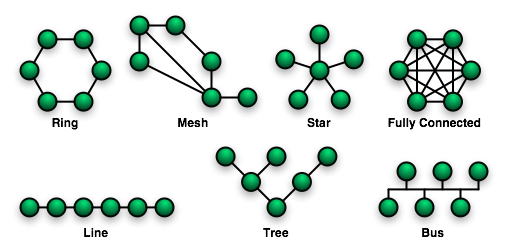
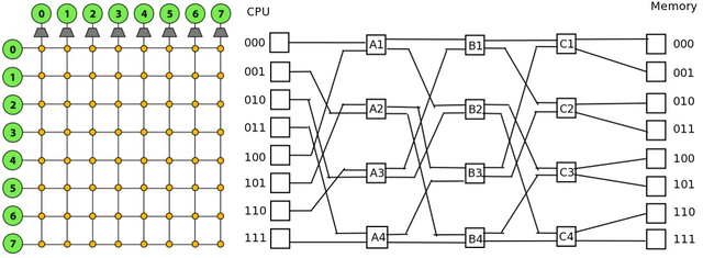
A network operation mode can be synchronous or asynchronous, the control can be centralized or distributed, and the switching can be packet switching or circuit switching. Packet switching doesn’t need to establish physical path between source and destination, it has packet with a header of source and destination address, it has routing information, it’s encapsulated (like an envelope of a letter), and available for short message. Mean while circuit switching establish physical path between source and destination, keep alive physical path during communication, high-speed bulk data transfer, and usually used in telephone communication. A network can be static (point-to-point) like topology of mesh, bus, star, ring, and tree on Figure 2. A network can be dynamic like a crossbar, and omega, on Figure 3. Either way a network usually have the following properties of diamiter, relay, node degree, and broadcast.

Figure 2. Static Network Topologies (https://upload.wikimedia.org/wikipedia/commons/9/96/NetworkTopologies.png)

Figure 3. Crossbar and Omega Network Topology (http://15418.courses.cs.cmu.edu/spring2013content/article_images/30_3.jpg and https://upload.wikimedia.org/wikipedia/commons/8/81/Omega_network.png)
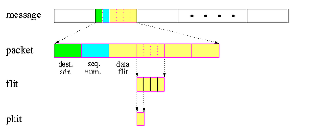
How messages were passed? In this context the structure of message is message, packet, flit, on Figure 4, which each packet contains data, sequence number, and address on one flit each. The routing method we used here are store and forward routing where the messages are broken into packets and sent and reconstruct the received packets back into messages on the receiver. Another one is wormhole routing that transfers flits by pipeline manner (note that packets can be broken into flits). Figure 5 shows the difference between store and forward routing between wormhole routing.

Figure 4. Message Structure (http://pages.cs.wisc.edu/~tvrdik/7/html/gif/units.gif)
Figure 5. Store & Forward, and Wormhole Routing (http://cnx.org/resources/32243490c16ba4eaebd5c34fe06fcf4e854607d0/graphics32.jpg)
However, a problem may occur when using wormhole routing which is a deadlock on Figure 6. This can a occur when no flits can proceed towards their destination because the buffer are full. A deadlock can be avoided using virtual channels, or flow control. The flow control method can be virtual cut-through routing which had flit buffer and packet buffer and uses 2 modes, it will use wormhole routing normally, but when a jam occurs it uses store and forward routing. Other methods are blocking where a gate placed on the transmission line to control the flow, the gate can either discard and retransmit when anomaly occurs or detours the transmission by means of adaptive routing (take a round trip).
Figure 6. Deadlock (http://cnx.org/resources/03fb3992e31cc435ef70d2406cf1da0833def44b/graphics30.jpg)
Mirrors
- https://www.publish0x.com/fajar-purnama-academics/my-summary-and-most-interested-topic-in-advanced-computer-or-xqogzkw?a=4oeEw0Yb0B&tid=github
- https://0darkking0.blogspot.com/2020/11/my-summary-and-most-interested-topic-in.html
- https://0fajarpurnama0.medium.com/my-summary-and-most-interested-topic-in-advanced-computer-organization-2-masters-course-1f20d0bea4a9
- https://0fajarpurnama0.github.io/masters/2020/10/13/summary-most-interested-topic-advanced-computer-organization-2-master-course
- https://hicc.cs.kumamoto-u.ac.jp/~fajar/masters/summary-most-interested-topic-advanced-computer-organization-2-master-course
- https://steemit.com/technology/@fajar.purnama/my-summary-and-most-interested-topic-in-advanced-computer-organization-2-master-s-course?r=fajar.purnama
- https://hive.blog/technology/@fajar.purnama/my-summary-and-most-interested-topic-in-advanced-computer-organization-2-master-s-course?ref=fajar.purnama
- https://blurt.buzz/blurtech/@fajar.purnama/my-summary-and-most-interested-topic-in-advanced-computer-organization-2-master-s-course?referral=fajar.purnama
- https://0fajarpurnama0.wixsite.com/0fajarpurnama0/post/my-summary-and-most-interested-topic-in-advanced-computer-organization-2-master-s-course
- http://0fajarpurnama0.weebly.com/blog/my-summary-and-most-interested-topic-in-advanced-computer-organization-2-masters-course
- https://0fajarpurnama0.cloudaccess.host/index.php/9-fajar-purnama-academics/114-my-summary-and-most-interested-topic-in-advanced-computer-organization-2-master-s-course
- https://read.cash/@FajarPurnama/my-summary-and-most-interested-topic-in-advanced-computer-organization-2-masters-course-b59a00b0
- https://www.uptrennd.com/post-detail/my-summary-and-most-interested-topic-in-advanced-computer-organization-2-master-s-course~ODE3NDIw


